| PREVIOUS PRESENTATION | BACK TO PROGRAM OVERVIEW | NEXT PRESENTATION |
Atomic-scale terahertz time-domain spectroscopy
V. Jelic, S. Adams, M. Hassan, K. Cleland-Host, S. Eve Ammerman, and Tyler L. Cocker
Department of Physics and Astronomy, Michigan State University, East Lansing, MI 48824 USA
Terahertz time-domain spectroscopy (THz-TDS) is one of the central technologies of THz science. By measuring the oscillating THz electric field after it has interacted with a sample and comparing it to a reference field, the complex dielectric function at THz frequencies may be determined. Based on the same concept, in THz scattering-type scanning near-field optical microscopy (s-SNOM), THz pulses focused onto a scanning probe tip may be used to spatially map the local complex dielectric function on the 10-100 nm scale [1]. However, many open questions in surface science require these properties to be determined at yet smaller length scales. For example, THz-TDS of individual atomic sites would allow the role of defects, dopants, and interfaces on charge transport to be studied in unprecedented detail.
Here, we introduce an experimental method for atomic-scale THz-TDS in a THz scanning tunneling microscope (THz-STM) junction. Using our technique, we demonstrate atomically resolved THz-TDS of a silicon-doped GaAs(110) sample, revealing a resonator defect with the hallmarks of the elusive DX center [2].
Fig. 1a shows a schematic of the THz-STM setup. A strong-field THz pulse is coupled to the STM tip and acts as an ultrafast bias voltage in the tip-sample junction, inducing a current pulse with a rectified component that is measured electronically [3]. To perform atomic-scale THz-TDS, we use this induced current pulse to sample a second, weaker THz pulse through a cross-correlation (THz-CC) measurement that captures the near-field waveform. In Fig. 1b, a THz-CC waveform is recorded on an Au(111) surface, which is used as a reference sample because of its flat spectral response. The spectrum of the near-field waveform is displayed in the inset. Fig. 1c shows an STM topography image of our GaAs(110) sample surface; the atomic rows are visible, as are multiple types of atomic defects (e.g., gallium vacancies and silicon substitutional dopants). The inset of Fig. 1c shows a high-resolution THz-STM image of the blue square region, where a particular defect exhibits a strong THz-STM signal.
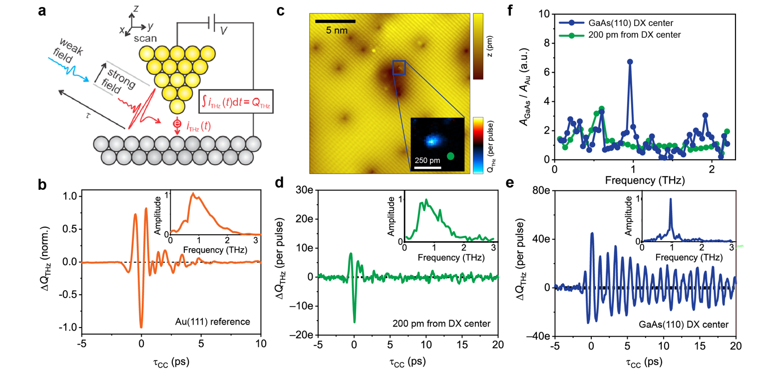
Figure 1: Terahertz time domain spectroscopy of a GaAs(110) surface on the atomic scale. a, Schematic of atomic-scale THz-TDS based on THz-STM, where a strong-field THz pulse induces a tunnel current that samples the oscillating field of a weak-field THz pulse in the tunnel junction through a cross-correlation (THz-CC) measurement. b, THz-CC waveforms measured on a reference Au(111) sample. Inset: Amplitude spectrum of the near-field waveform on Au(111). c, STM topography image of the GaAs(110) surface, with atomic rows and multiple types of defects visible. Inset: THz-STM image of a small region of the STM image (blue square), which contains a strong and highly localized THz-STM signal. d,e, THz-CC waveforms measured on the GaAs(110) surface 200 pm away from the bright defect (d), which is indicated by a green circle in the inset of c, and on the prominent THz-STM feature, which is associated with a DX center (e). Insets show the normalized spectrum of the respective near-field waveform. f, Amplitude spectra of d and e divided by the gold reference spectrum (inset of b).
Near-field waveforms were measured 200 pm away from the defect (Fig. 1d; green circle in Fig. 1c) and in the center of the bright feature in the THz-STM scan (Fig 1e). In Fig. 1f, we divide the amplitude spectra of the GaAs(110) near-field waveforms (insets in Fig. 1d and e) by the Au(111) reference spectrum (inset of Fig 1b). The distinct responses for the two sample locations are due to dielectric contrast. Spectroscopically, the most prominent contrast occurs at 0.96 THz, where the defect exhibits a strong resonance that is absent at the location 200 pm away. From this signature resonance and other STM characteristics (not shown), we identify the defect as a silicon-vacancy complex stabilized in a DX center configuration and the resonance as the vibrational motion of the silicon dopant atom. Although DX centers are of significant interest in semiconductor research due to their prominent role in carrier scattering [4], this is the first time one has been observed directly.
With atomic-scale THz-TDS we can now study open questions that previously could not be addressed experimentally, such as the simultaneous spatial and spectral description of defect complexes in semiconductors. As a next step, we envision that THz-TDS within a THz-STM junction will enable time-resolved THz spectroscopy of the transient THz dielectric response on the atomic scale.
References
[1] T. L. Cocker, V. Jelic, R. Hillenbrand and F. A. Hegmann, “Nanoscale terahertz scanning probe microscopy,” Nat. Photon. 15, 558–569 (2021)
[2] V. Jelic, S. Adams, M. Hassan, K. Cleland-Host, S. E. Ammerman and T. L. Cocker, “Atomic-scale terahertz time-domain spectroscopy,” submitted.
[3] T. L. Cocker, V. Jelic, M. Gupta, S. J. Molesky, J. A. J. Burgess, G. De Los Reyes, L. V. Titova, Y. Y. Tsui, M. R. Freeman and F. A. Hegmann, “An ultrafast terahertz scanning tunnelling microscope,” Nat. Photon. 7, 620–625 (2013)
[4] A. Kundu, F. Otte, J. Carrete, P. Erhart, W. Li, N. Mingo and G. K. H. Madsen, “Effect of local chemistry and structure on thermal transport in doped GaAs,” Phys. Rev. Mater. 3, 094602 (2019)