| PREVIOUS PRESENTATION | BACK TO PROGRAM OVERVIEW | NEXT PRESENTATION |
Unravelling Topographic Contrast from THz-SNOM Data of Semiconductor Nanowires
W. V. Carstensen1, G. Meucci2, D. Beznasiuk2, T. S. Jespersen2, S. J. Lange1, P. U. Jepsen1, and E. J. R. Kelleher1
1Department of Electrical and Photonics Engineering, Technical University of Denmark, Ørsteds Plads 343, 2800 Kgs. Lyngby, Denmark
2Department of Energy Conversion and Storage, Technical University of Denmark, Anker Engelunds Vej 301, 2800 Kgs. Lyngby, Denmark
Nanoelectronics technology has become increasingly miniaturized, necessitating fabrication techniques for producing large quantities of sub-micron structures at high speeds. These structures require nanoscale characterization to ensure quality [1]. Terahertz (THz) scattering-type scanning near-field optical microscopy (THz-SNOM) can probe material properties far below the diffraction limit of the corresponding free-space THz light, providing information on variations in conductivity and permittivity at spatial resolutions on the nanoscale [2]. However, non-flat structures with topographic features with dimensions on the order of the scanning probe tip can cause variations in the SNOM signal unrelated to contrast induced by changes to the local material properties. Furthermore, widely used models for the interpretation of SNOM data are optimized for extended layered material stacks, where structural variations exist only in the out-of-plane direction. This abstract explores topography-induced artifacts in THz-SNOM data of semiconducting nanowires and suggests strategies to mitigate them to reveal local variations in contrast dominated by the material properties.
THz-SNOM is a modified tapping-mode AFM illuminated by a pulsed THz light source. The strength of the scattered signal detected as a function probe-sample height depends on the interaction between the tip and its dielectric environment. The recorded signal is demodulated at the tip tapping frequency and normalized by the demodulated signal on the substrate: ηi = Sisample/Sisub, where ηi is the contrast of the i-th demodulation order, generally proportional to the sample’s conductivity. The sample is a semiconductor nanowire with a triangular cross-section (as shown schematically in Figure 1(a)). For reference, an identical sample with an Au layer of 20 nm on top was considered. The semiconductor nanowire was expected to have higher conductivity than the substrate, while the Au-coated sample should have uniform conductivity in the plane.
Initial scans show lower signals on the wires than on the substrate due to topography. The 2D maps of the demodulated signals (η2, η3, η4 and η5) are shown in Fig. 1(b). Figures 1(c) and 1(d) show the average of the contrast along the length of the wire for the two samples as well as the order-normalized contrast. [3] The topographically induced artifacts are caused by both changing interaction between the tip and the substrate, as well as the mechanical changes in the AFM, which occur on slopes and changing interaction area with the tip [4].
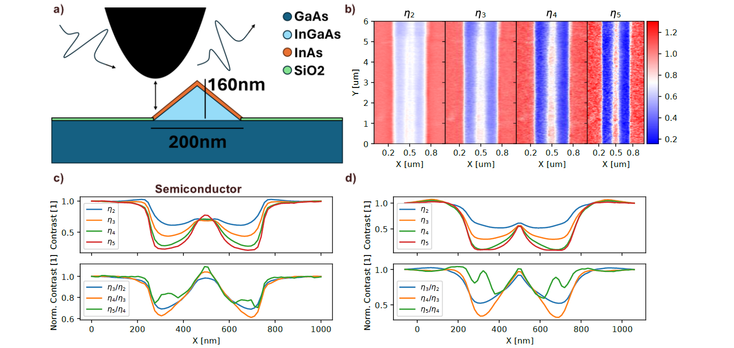
Figure 1: a) Shows schematic of a slice of the semiconductor nanowire including the tip of the SNOM which is modulated vertically. b) shows a 1×6 micron scan of a nanowire resolved at four demodulated orders normalized by the substrate. c) shows the average contrast along the wire for the demodulated signal as well as the average of the order-normalized contrast. d) shows the same type of results as c) but for an identical measurement of the Au-coated wire.
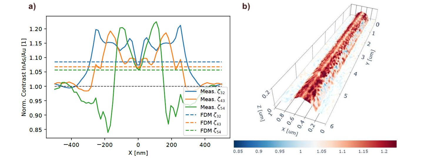
Figure 2: a) Shows the InAs order-normalized contrast divided by the order-normalized contrast on the Au coated wire. The black dashed line is a guide to the eye for contrast 1. The three upper dashed lines indicate the order-normalized values calculated using FDM of the InAs, InGaAs, GaAs stack. b) shows the topography of the wire measured by AFM with the colour scale being the average order-normalized map of InAs divided by the average line correction of the Au coated wire.
Most artifacts occur due to the wire’s slope or proximity, but at the wire’s apex, the topography’s derivative is zero. Comparing the semiconductor nanowire signal to the Au-coated wire signal—representing a pure topographic signal—can reveal material properties. Note that different tips used for comparison introduce varying topographic artifacts on the slope of the wire, though qualitatively similar. The comparison is performed by dividing the order-normalized contrasts of the semiconductor sample and the topographic sample, essentially scaling the values by the topographic impact: ζij = ηijInAs/ηijAu. The resulting values are shown in Fig. 2(a). The overall signal varies across the wire, due to the different tip impacts, but is constant near the top for any selection of orders. The correction can be done for a combination of the order-normalized values and used to correct a combination of the maps. This is shown in Fig. 2(b), revealing a lower scattering from the substrate, sloped areas expressing the residual topographic artefacts, and a high signal on the crest of the wire, demonstrating a clear longitudinal variation of signal, which we attribute to local changes in the material properties. Calculation of the magnitude of the expected scattering signal using the extended finite dipole model (FDM) for a layered system provides an estimate of the expected contrast, which we find to be in good agreement with our experimental results. Ultimately this procedure could be applied to relate measured contrast to nanoscale variations in carrier concentration. We believe our work lays the foundation for the development of methods to unravel the material properties of topographically non-trivial nanoscale structures characterised using THz-SNOM.
References
[1] D. V. Beznasyuk, S. Martí-Sánchez, J.-H. Kang, R. Tanta , M. Rajpalke, T. Stankevic , A. W. Christensen, M. Ch. Spadaro , R. Bergamaschini, N. N. Maka, C. E. N. Petersen, D. J. Carrad, T. S. Jespersen, J. Arbiol, and P. Krogstrup, “Doubling the mobility of InAs/InGaAs selective area grown nanowires,” Phys. Rev. Materials 6, 034602 (2022)
[2] X. Guo, K. Bertling, B. C. Donose, M. Brunig, A. Cernescu, A. A. Govyadinov, and A. D. Rakic, “Terahertz nanoscopy: Advances, challenges, and the road ahead,” Appl. Phys. Rev. 11, 021306 (2024)
[3] L. Mester, A. A. Govyadinov and R. Hillenbrand, “High-fidelity nano-FTIR spectroscopy by on-pixel normalization of signal harmonics,” Nanophotonics 11, 377 (2022)
[4] M. Stark, C. Möller, D. J. Müller, and R. Guckenberger, “From Images to Interactions: High-Resolution Phase Imaging in Tapping-Mode Atomic Force Microscopy,” Biophys. J. 80, 3009 (2001)