| PREVIOUS PRESENTATION | BACK TO PROGRAM OVERVIEW | NEXT PRESENTATION |
Terahertz response of 3D graphene aerogels
P. Kumar, M. Šilhavík, M. R. Parida, H. Němec, J. Červenka, and P. Kužel
FZU – Institute of Physics of the Czech Academy of Sciences, Na Slovance 2, Prague 8 18221, CZ
Graphene has emerged as an outstanding two-dimensional (2D) material due to its unique optical and electronic properties such as high electron mobility, charge-density tunability, highly nonlinear terahertz response etc. In recent years, thanks to the development of graphene synthesis, 3D graphene networks assembled in free-standing covalently cross-linked graphene aerogel (GA) structures that maintain the characteristic properties of single-layer/multilayer graphene have been realized. Compared with traditional 2D graphenes, GAs provide high porosity and large effective surface area (Fig. 1a) and they are also lightweight (ρ ∼ 6 mg/cm3), elastic, and mechanically robust, making them promising for various applications, e.g., strain and pressure sensing [1].
In the first part of this talk we will present and discuss a systematic study of steady-state THz conductivity and permittivity in GA (in the range 0.15–10 THz) and of its ultrafast response to the optical excitation. The experiments reveal an interplay between the Drude and hopping conductivity (Fig. 1b), which is significantly different from the transport observed in 2D graphene layers. The hopping process controls the transport in defect-rich parts of the 3D graphene networks; conversely, the parts with low defect concentration are dominated by the Drude band-like conductivity. An interplay between the two mechanisms can be tuned by the annealing temperature of the structures [2].
This technological process can also be used for tuning the optical properties of 3D graphene in the THz range. Indeed, the refractive index of the foam-like structure of GAs is close to unity and ensures a very low impedance mismatch with the surrounding air for freely propagating THz radiation. The annealing process then allows one to switch the material optical properties in an ultrabroadband THz range (Fig. 1c) from a stealth element (low temperature annealing, 𝑅 < 1%), to THz absorber (annealing at medium temperature, 𝐴 > 85%) and to a shielding element (high temperature annealing, 𝑇 < 0.1%) [3].
Finally, the talk will discuss the modulation of the THz opto-electronic properties of 3D graphene by an applied static and/or dynamical strain (straintronics, Figs. 1a,d). It has been previously shown that 3D graphene is able to sustain reversible elastic deformation exceeding ~ 90% without structural failure [4]. Below a certain linear strain threshold (γt ≈ 50%) the THz conductivity and permittivity are simply proportional to the graphene filling fraction and, thus, the conductivity mechanisms and current pathways remain the same within this deformation regime. As the strain increases above γt a nonlinear regime is set up associated with structural changes in the sample confirmed by SEM pictures. In this regime, the pores in the 3D graphene deform significantly and new conductive channels progressively appear due to the pore buckling; the multiplication of electrical conducting paths drives the sample into a superlinear straintronic regime where defect-rich parts are bypassed by newly created channels with band-like conductivity. The interaction of THz radiation with the sample under the strain can be also modulated dynamically at kHz frequencies by an application of suitable piezo-elements [5].
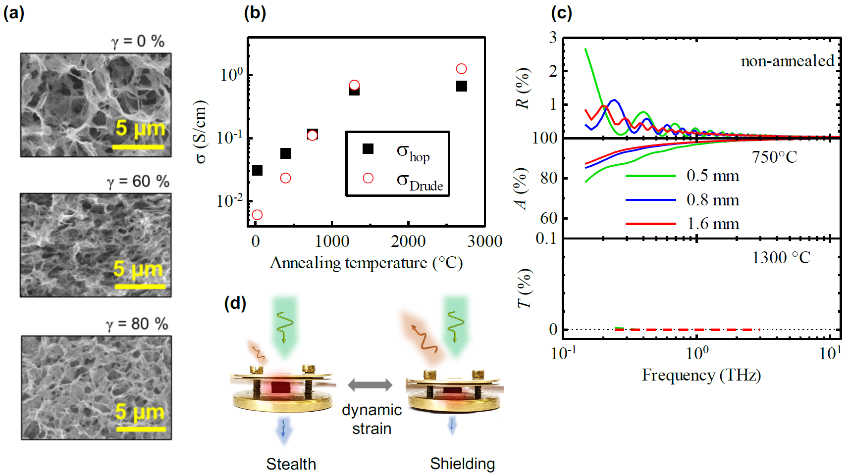
Figure 1: (a) Scanning electron micrographs of a 3D graphene sample: unstrained (γ = 0%) and submitted to γ = 60% and 80% strain. (b) Hopping (σhop) and Drude (σDrude) contributions to the THz conductivity as a function of the annealing temperature (without strain). (c) THz properties of variously annealed samples with three different thicknesses: reflectivity of a non-annealed sample, absorptivity of a sample annealed at 750 °C and transmissivity of a sample annealed at 1300°C. (d) Scheme of a straintronic device in an unstrained and strained state.
References
[1] S. Luo, Y. A. Samad, V. Chan and K. Liao, Matter 1, 1148 (2019)
[2] P. Kumar, M. Šilhavík, M. R. Parida, H. Němec, J. Červenka, and P. Kužel, Nanoscale Adv. 5, 2933 (2023)
[3] P. Kumar, M. Šilhavík, J. Červenka, and P. Kužel, J. Phys. D. Appl. Phys. 56, 505103 (2023)
[4] M. Šilhavík, P. Kumar, Z. A. Zafar, M. Míšek, M. Čičala, M. Piliarik, and J. Červenka, Commun. Phys. 5, 27 (2022)
[5] P. Kumar, M. Šilhavík, M. R. Parida, P. Kužel, and J. Červenka, Adv. Electron. Mater. (2024), https://doi.org/10.1002/aelm.202300853