| PREVIOUS PRESENTATION | BACK TO PROGRAM OVERVIEW | NEXT PRESENTATION |
Terahertz Emission Spectroscopy and Imaging as a Quantitative Analytical Tool
Masayoshi Tonouchi
Osaka University, Japan
Terahertz emission spectroscopy (TES) has been used for many years to explore photocarrier dynamics in various electronic materials [1]. Although TES utilizes the same system for THz time-domain spectroscopy (THz-TDS), they provide completely different information on material properties. THz-TDS has established itself as a tool to estimate the refractive index of materials, whereas TES discusses the THz excitation mechanism upon femtosecond laser illumination from various materials phenomenologically, which is now recognized as a powerful tool to explain the ultrafast photocarrier dynamics [2-6]. However, this “phenomenological” feature has conversely hindered the widespread use of TES. For the market development of TES, it should evolve into a versatile tool by providing the quantitative parameters of the materials. Thus, recently, we have focused on this point. We have proven that one can extract the various parameters of semiconductors from the TES data, which extends the market into semiconductor R&D. Examples are the parameter extraction for Si-wafer, p-n junctions, MOS, wide bandgap semiconductors, and so on [7-12]. Figure 1 shows the schematics for photoresponse near the surface of a semiconductor. By simplifying the emission mechanism [7], one can estimate its surface potential from the emission data in a wafer scale noncontactly and non-destructively. This analysis is sensitive enough to assess the potential change due to the surface dipole formation during surface treatment with BHF. In the presentation, we introduce such performance as a quantitative analytical tool.
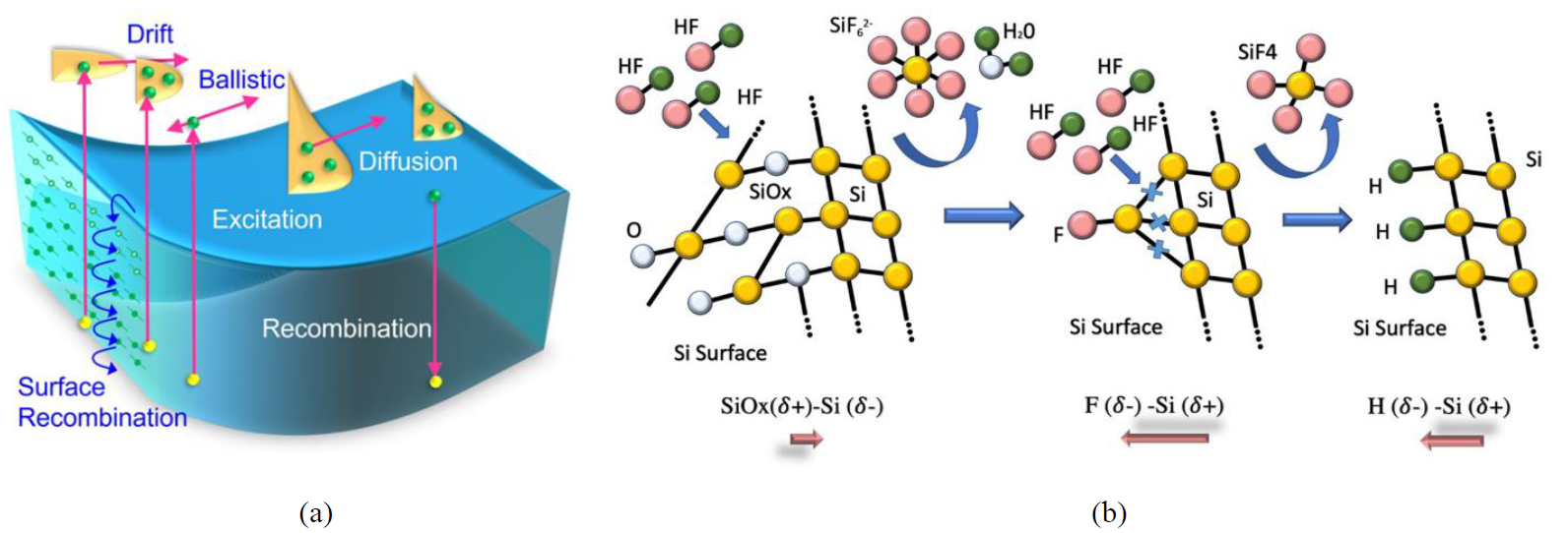
Figure 1: (a) Photo excitation followed by the carrier displacement to generate THz waves. (b) BHF etching modifies the strength of the surface dipoles at the Si surface bonded with oxygen, fluorine, and hydrogen.
Acknowledgments
M.T. acknowledges support in part by JSPS KAKENHI Grant No. JP23H00184.
References
[1] A. Leitenstorfer, et al., “The 2023 terahertz science and technology roadmap”, Journal of Physics D: Applied Physics 56, 223001 (2023)
[2] D.S.Rana, M.Tonouchi, “Terahertz Emission Functionality of High Temperature Superconductors and Similar Complex Systems,” Advanced Optical Materials 8, 1900892 (2020).
[3] K.J.P. Jacobs et al., “Characterization of through-silicon vias using laser terahertz emission microscopy,” Nature Electronics 4, 202 (2021)
[4] A. Mannan et al., “Ultrafast Terahertz Nanoseismology of GaInN/GaN Multiple Quantum Wells,” Advanced Optical Materials 9, 2100258 (2021).
[5] F. Murakami et al., “Probing photocarrier dynamics in a Bi2Te3-Te eutectic p-n junction with a laser terahertz emission microscope”, APL Materials 11, 031102 (2023)
[6] M. Wais et al., “Transition from Diffusive to Superdiffusive Transport in Carbon Nanotube Networks via Nematic Order Control,” Nano Letters 23, 4448 (2023)
[7] D. Yang et al., “Rapid, noncontact, sensitive, and semiquantitative characterization of buffered hydrogen-fluoride-treated silicon wafer surfaces by terahertz emission spectroscopy,” Light: Science & Applications 11, 334 (2022)
[8] D. Yang et al., “Noncontact evaluation of the interface potential in VO2/Si heterojunctions across metal–insulator phase transition”, Applied Physics Letters 122, 041601 (2023)
[9] K. Suzuki et al., “Noncontact measurement of dopant depth profile with terahertz emission spectroscopy,” Metrology, Inspection, and Process Control XXXVIII; 1295506 (2024); F. Murakami et al., in preparation.
[10] D. Yang D., M. Tonouchi, “Understanding terahertz emission properties from a metal-insulator-semiconductor structure upon femtosecond laser illumination,” Journal of Applied Physics 130, 55701 (2021)
[11] D. Yang, M. Tonouchi, “Quantifying Flat-Band Voltage in Si Metal-Oxide-Semiconductor Structures: An Evaluation via Terahertz Emission Spectroscopy (TES), ” International Journal of High Speed Electronics and Systems, 2440018 (2024).
[12] F. Murakami et al., “Enhanced luminescence efficiency in Eu-doped GaN superlattice structures revealed by terahertz emission spectroscopy”, Communications Materials 4, 100 (2023)